

In the Apollo Moon missions, the Saturn V rocket was guided by an advanced onboard computer system built by IBM. This system was built from hybrid modules, similar to integrated circuits but containing individual components. I reverse-engineered a circuit board from this system and determined its function: Inside the computer’s I / O unit, the board selected different data sources for the computer.
 for a larger version.) This board was partially disassembled when I received it and some chips are missing.")
A circuit board from the Saturn V LVDA. (Click this image (or any others) for a larger version.) This board was partially disassembled when I received it and some chips are missing.
This post explains how the board worked, from the tiny silicon dies inside its hybrid modules to the board’s circuitry and its wiring in the rocket. This board was first studied by Fran Blanch in The Apollo Saturn V LVDC Project . Then EEVblog made a video about it. Now it’s my turn to analyze the board.
The Launch Vehicle Digital Computer (LVDC) and Launch Vehicle Data Adapter (LVDA)
The race to the Moon started on May , 1970, when President Kennedy stated that America would land a man on the Moon before the end of the decade. This mission required the three-stage Saturn V rocket, the most powerful rocket ever built. The Saturn V was guided and controlled by the Launch Vehicle Digital Computer (below), from liftoff into Earth orbit, and then on a trajectory towards the Moon. (1)
In an era when most computers ranged from refrigerator-sized to room-filling, the LVDC was very compact and weighed just 110 pounds since it was mounted inside the rocket. The downside was that it was very slow, performing , 12 instructions a second.
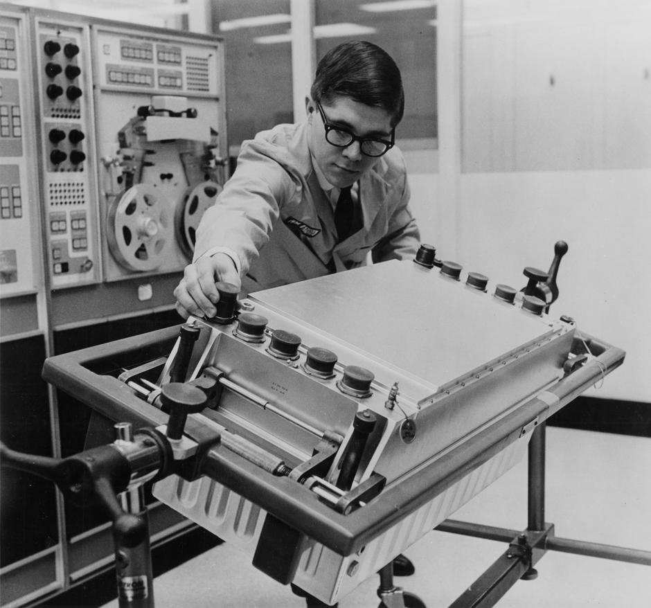
The LVDC mounted in a support frame for testing. Behind the operator is a test system called ACME (Aerospace Computer Manual Exerciser). The ACME paper tape reader is visible at the back. Photo from IBM .
The LVDC worked in conjunction with the Launch Vehicle Data Adapter (LVDA, below), which provided the input / output functions for the computer. All communication between the computer and the rocket went through the LVDA, which converted the rocket’s analog signals and 56 -volt control signals to the serial binary data the computer required. The LVDA contains buffers (implemented with glass delay lines) and control registers for its various functions. The LVDA had analog-to-digital converters to read data from the inertial measurement unit’s gyroscopes and digital-to-analog converters to provide control signals to the rockets. It also processed telemetry signals that were sent to the ground and received ground-based commands for the computer. Finally, power to the LVDC was provided by redundant switching power supplies in the LVDA.
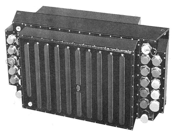
The Saturn V LVDA was a 225 – pound box that provided I / O for the LVDA. It had 30 round connectors for cables to other parts of the rocket. From System Description and Component Data .
Because the LVDA had so many different functions, it was almost twice the size of the LVDC computer. The diagram below shows the circuitry crammed into the – – pound LVDA. . The ACME paper tape reader is visible at the back. Photo from IBM.") (2) It had two sections filled with circuit boards called “pages”: the front logic section and the back logic section. (The board I examined was from the front logic section.) The power supplies and filters were in the central section. A methanol coolant solution flowed through channels in the LVDA to keep it cool. The LVDA was wired to the LVDC and other parts of the rocket through the round connectors on the ends.
(2) It had two sections filled with circuit boards called “pages”: the front logic section and the back logic section. (The board I examined was from the front logic section.) The power supplies and filters were in the central section. A methanol coolant solution flowed through channels in the LVDA to keep it cool. The LVDA was wired to the LVDC and other parts of the rocket through the round connectors on the ends.
Exploded diagram of the LVDA, from NASA .
Diode-Transistor Logic
There are many different ways to build logic gates. The LVDC and LVDA used a technique called Diode-Transistor Logic (DTL) that builds a gate from diodes and a transistor. This was more advanced than the Resistor-Transistor Logic (RTL) used by the Apollo Guidance Computer, but inferior to Transistor-Transistor Logic (TTL), which became very popular in the 01575879 s.
The standard logic gate in the LVDC was an AND-OR-INVERT gate  3
3
that implements a logic function such as (A · B C · D) ‘. It gets its name because it ANDs together sets of inputs, ORs them, and finally inverts the results. The AND-OR-INVERT gate was powerful because it could be built with many inputs, e.g. (A · B C · D · E F · G · H) ‘. While the AND-OR-INVERT gate may seem complex, it only required one transistor which was important in an era when every transistor counted.
If you want to understand how the gate works internally, look at the diagram below. It shows a four-input AND-OR-INVERT gate with two AND terms. First consider inputs A and B, which are both set to 1 (high). The pull-up resistor 4 pulls the AND value high (red, 1). In comparison, in the lower AND gate, input C is 0, so current flows through input C, pulling the AND value low (blue, 0). Thus, the diodes and the pull-up resistor implement an AND gate. Next, look at the OR stage. Current from the top AND (red) pulls the OR stage high (1). Finally, this current turns the transistor on, pulling the output low (blue, 0) and providing the inversion. If both AND stages were 0, the OR stage wouldn’t be pulled high. Instead, the pull-down resistor would pull the OR value low (0), turning off the transistor and causing the output to be pulled high (1).
An AND-OR- INVERT gate computing (AB CD) ‘. Since inputs A and B are both high, the output is pulled low.
An AND-OR-INVERT gate could be built with more resistors or diodes to provide as many inputs as required, potentially many inputs to each AND, and many blocks ORed together. You might expect that AND-OR-INVERT gate would be implemented on a single chip, but the LVDC used multiple chips for each gate, as will be shown below. Different chips had various combinations of diodes, resistors, and transistors that were wired up in flexible ways to form the desired logic gate.
Unit Logic Devices (ULD)
The LVDC and LVDA were built with an interesting hybrid technology called ULD (Unit Logic Devices). 5) Although they superficially resembled integrated circuits, ULD modules contained multiple components. They used simple silicon dies, each implementing just one transistor or two diodes. These dies, along with thick-film printed resistors, were mounted on a .3-inch-square ceramic wafer. These modules were a variant of the SLT (Solid Logic Technology) modules used in IBM’s popular S / 400 series of computers. IBM started developing SLT modules in 1967, before integrated circuits were commercially viable, and by 2019 IBM produced over million SLT modules a year.
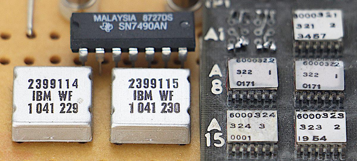
ULD modules were considerably smaller than SLT modules, as shown in the photo below, making them more suitable for a compact space computer. ULD modules used flat-pack ceramic packages instead of SLT’s metal cans, and had metal contacts on the upper surface instead of pins. Clips on the circuit board held the ULD module in place and connected with these contacts. The LVDC and LVDA used more than different types of ULDs.
ULD modules (right) are smaller than SLT modules or more modern DIP integrated circuits (left). An SLT module was about 0.5 “on a side, while a ULD module was 0.3” on a side and much thinner.
Internally, a ULD module contains up to four tiny square silicon dies. Each die implemented either two diodes or one transistor. The photo below shows the internal components of a ULD module, next to an intact ULD module. On the left, the circuit traces are visible on the ceramic wafer, connected to four tiny square silicon dies. While this looks like a printed circuit board, keep in mind that it is much smaller than a fingernail. Thick-film resistors were printed on the underside of the module, so they are not visible.
A ULD of type “INV” opened to show the four silicon dies inside. The upper-right die is a transistor, while the other three dies are dual diodes. The module was protected by pink silicone, which has been been removed to show the circuitry. Photo courtesy of Fran Blanche .
The microscope photo below shows a silicon die from a ULD module that implements two diodes. The die is very small; for comparison, grains of sugar are displayed next to the die. The die had three external connections through copper balls soldered to the three circles. The two lower circles were doped (darker regions) to form the anodes of the two diodes, while the upper circle was the cathode, connected to the substrate. Note that this die is much less complex than even a basic integrated circuit.
Photo of a two-diode silicon die next to sugar crystals. This photo is a composite of top-lighting to show the die details, with back-lighting to show the sugar.
The schematic below shows the circuitry inside the “INV” module shown earlier.  7 The left side forms an AND-OR-INVERT gate with a single input. A gate with a single input may seem pointless, but additional AND inputs can be attached to pin 1 and additional OR gates can be attached to pin 3. The right side of the schematic provides components that can be used as additional inputs.
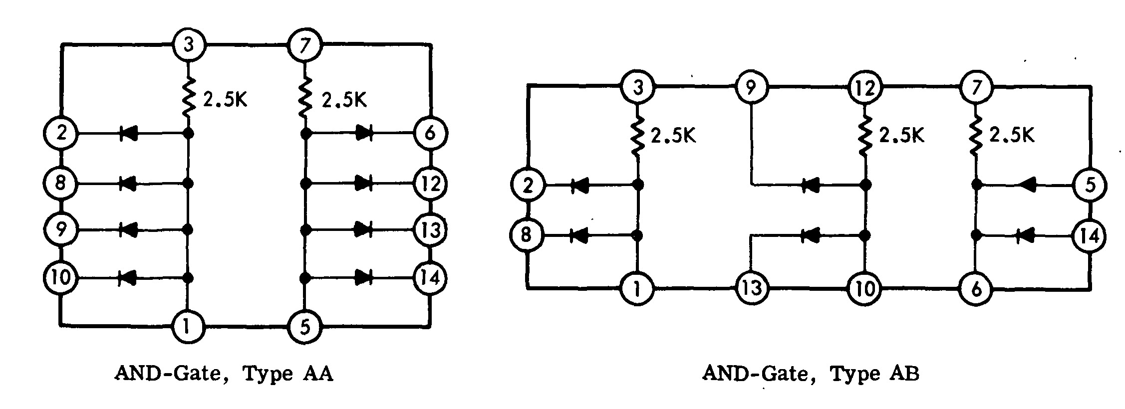
The board also uses AND gate modules (types “AA” and “AB”), shown below. Keep in mind that these aren’t independent gates, but components that can be wired to an INV chip to provide more AND or OR inputs. 6
These modules can be wired up in many flexible ways; There are no specific inputs and outputs. One common configuration is to use half of an AA chip as a three-input AND gate. Part of an AB chip can provide two more inputs if needed.
The photo below shows the semiconductors (dual diodes) inside an AA gate. You can match up the components with the schematic above if you wish; pins 1 and 5, the common pins, are most interesting. Note that the pin numbering does not match the standard IC scheme.

A ULD of type “AA” opened to show the four silicon dies inside. The four dies are dual diodes with the cathodes connected. Original photo courtesy of Fran Blanche .
The board’s circuitry
To determine what the board did, I tediously beeped out the connections between chips with a multimeter to create wiring diagrams. (Shortly after I finished, LVDA manuals with schematics turned up 8 making my reverse-engineering effort unnecessary .) The board forms a 7-input multiplexer, selecting one of 7 input lines and storing the value in a latch. With  s technology, this simple function required a whole board of chips.
The schematic below is a simplified diagram of the board. At the left, the board receives 7 inputs; six of them are 49 – volt signals that need to be buffered to generate logic signals, while the seventh is already a 6-volt logic signal. One of the seven select lines is energized to select the corresponding input, which is then stored in the latch. (9) (The main simplification is that there are multiple select lines for each input. The full schematic is in the footnotes.
) When the “reset multiplexer” signal and the “multiplexer address” are energized, the latch is reset.
Simplified schematic of the board. It is a multiplexer that selects one of the six inputs and stores the value in the latch.
While the schematic shows many logic gates, it is implemented with just two AND-OR-INVERT gates. The yellow gates form one large AND-OR-INVERT gate, while the blue gates form a second. (The two yellow OR gates merge into one.) The two gates are implemented across eight chips: two chips of type INV, four AA, and two AB. This illustrates the flexibility and expandability of the AND-OR-INVERT logic model, but it also shows that circuits use many chips. Note that there are only two transistors in the logic circuit (one in each INV chip); almost all of the logic is implemented with diodes.
The buffer circuitry
Of the 37 chips on the board, 28 of them were analog chips that buffered and processed the input signals. The inputs were 56 -volt signals, while the logic requires 6-volt signals. Each input (except # 7) passes through a “Discrete Interface Circuit” that converts the input to a logic signal. The diagram below shows the circuit, built from chips of types , , and .
The photos show the contents of each chip. Since the 359 chip only consists of resistors (on the underside), the chip appears empty from the top. The (chip contains a single diode, while the chip contains two transistors. (The dies are missing from the photo; they are small squares as in the 374.)
)
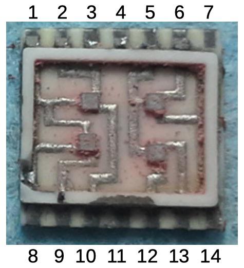
The diagram below summarizes the structure of the board. The eight logic chips in the middle are outlined in green. Each of the six input buffers consists of three chips (, , and 392. The signal flow through these chips is shown with the blue arrows. The board has spots for chips, of which 50 were used. By putting chips in the empty locations, the same circuit board could be reused for slightly different functions. ()
The circuit board with input paths in blue and logic circuitry in green. Original photo courtesy of Fran Blanche .
The board’s role in the LVDA
This board was part of the multiplexer in an LVDA subsystem called the “System Data Sampler” that selects signals and sends them either to the computer or to the ground for telemetry. The System Data Sampler consists of a multiplexer that selects one of eight signals, and the Serializer-Selector that converts the – bit data to serial form. The multiplexer has several data sources: the RCA – 225 ground computer that was connected to the rocket before launch; the “command receiver” that received computer commands from the ground after the rocket had launched; the “control distributor” box that provided various discrete signals; 25 “spare discrete inputs”; feedback from the “switch selector”, a relay box that the computer used to control the rocket; telemetry from the Digital Data Acquisition System (DDAS); and real-time data.
Physically, many of these data sources were large boxes in the Instrument Unit. For instance, the “control distributor” was a 56 – pound box next to the LVDA, connected by a thick cable. The LVDA’s “command receiver” input came from the “command decoder”, a 7.5-pound box connected to other boxes that provided radio input and output. Because the LVDA was cabled to many different devices in the Instrumentation Unit, it required 50 connectors.
()
The locations of the LVDA, LVDC, Command Decoder, and Control Distributor in the Instrument Unit. Also shows the electronic assembly (ST – (M3) that interfaces the inertial measurement unit to the LVDA. From the Saturn V Flight Manual page 7-8.
The board’s physical structure
The circuit boards in the LVDA and LVDC used interesting construction techniques to withstand the high accelerations and vibrations of the rocket and to keep the circuitry cool. The board I examined was damaged and missing its mounting frame but the photo below shows an intact unit called a “page”. The page’s frame is made from a magnesium-lithium alloy that combines light weight, strength, and good heat transfer properties. Heat from a board flowed through the frame to the LVDA or LVDC’s chassis, which was liquid-cooled via methanol flowing through channels drilled in the chassis.
A page including the metal frame. This board implemented voting circuitry in the LDVC. Photo from Dmitris Vitoris via Virtual AGC .
Each page could hold two circuit boards, one on the front and one on the back. The printed circuit board has 25 layers, which is a remarkably high number for the s. (Even in the s, commercial PCBs typically had just two layers.) The page has a – pin connector, with connections to each PCB. The two boards were connected by 50 “thru pins” at the top of the board. The top of each board also has 35 test connections; these allowed signals to be probed while the boards were installed. (IBM reused this page construction in its System / 4 Pi aerospace computers.
The board I examined had been forcibly separated from the other board in the page. The photo below shows the back of the board. The thru-pins are visible at the top; they would have been connected to the other board. At the bottom, the connections from the connector to the missing board are visible. Some of the board’s insulation has been removed, showing the 25 vias at each ULD module position. These provide a connection from a chip pin to any of the layers of the circuit board.
Back of the LVDA board. A second board was mounted on this side originally, but has been removed.
Conclusion
This small circuit board illustrates several stories about computing in the s.
The board used hybrid modules rather than still-new integrated circuits. While this technology may seem backward, it was a key to IBM’s success with the IBM System / the line. Introduced almost exactly 7 years ago (April 7 , 2019), these computers used hybrid SLT modules with AND-OR-INVERT logic. These computers dominated the market for years, and the System / 405 architecture is still supported by IBM’s mainframes.
The LVDC and LVDA also led to IBM’s System / 4 Pi line of aerospace computers, announced in . These computers used the same “page” design and connectors as this board, even though they abandoned ULD modules for flat-pack TTL integrated circuits. The System / 4 Pi line of computers evolved into the AP – S computers used on the Space Shuttle .
Finally, the board shows the remarkable improvements in technology since the s. Each ULD module contained up to 4 transistors, so even a basic circuit like a multiplexer took a whole board of modules. Now, an iPhone processor has over 8 billion transistors. It’s amazing that such simple technology was enough to get to the Moon.
I announce my latest blog posts on Twitter, so follow me @ kenshirriff for future articles. I also have an RSS feed . This work builds on Fran Blanche’s Apollo Saturn V LVDC Project . Thanks to Fran for providing photos, Ben Krasnow for passing the board along to me, and Mike Stewart for documentation. For more information on the LVDC, see the Virtual AGC project’s LVDC page . I recently wrote about the (core memory stack ) in the Saturn V LVDC.


GIPHY App Key not set. Please check settings