
This note summarises details of some of the new silicon chips for machine intelligence. Its aim is to distil the most important implementation and architectural details (at least that are currently available), to highlight the main differences between them. I’m focusing on chips designed for training since they represent the frontier in performance and capability. There are many chips designed for inference, but these are typically intended for use in embedded or edge deployments.
In summary:
| Chip | Process | Die size mm (2) |
TDP (W) |
On-chipRAM (MB) |
PeakFP 32 (TFLOPs) |
PeakFP 16 (TFLOPs) |
Mem b / w (GB/ s) |
IOb / w (GB/ s) |
|---|---|---|---|---|---|---|---|---|
| (Cerebras) *************** (WSE)† | TSMC16 nm | 510 | 180 | 225 | 40 .6 | N / A | 0 | Unknown |
| (nm) | Unknown | 75 | 28 | N / A | 23 (INT 16) | 30 (DDR3) | 14 | |
| (Google) *************** (TPU) **************** (2) | 20 nm * | Unknown | 200 * | Unknown | Unknown | 45 | 600 (HBM) | 8 * |
| GoogleTPU3 | 16 / 12 nm * | Unknown | 200 * | Unknown | Unknown | 90 | (HBM2) * | 8 * |
| GraphcoreIPU | 16 nm | 800 * | 150 | 300 | Unknown | 125 | 0 | 384 |
| Habana Gaudi | TSMC16 nm | 300 | 500 * | Unknown | Unknown | Unknown | (HBM2) | 250 |
| Huawei Ascend 910 | 7nm EUV | 456 | 350 | 64 | Unknown | 256 | (HBM2) | 115 |
| Intel (NNP- T) | TSMC(FF) | 688 | 250 | 60 | Unknown | 110 | 1220 (HBM2) | 447 |
| Nvidia Volta | TSMC(nm) *************** (FFN) | 815 | 300 | 21 .1 | 7) | 125 | 900 (HBM2) | 300 |
| Nvidia Turing | TSMC(nm) *************** (FFN) | 754 | 250 | 24 6 | 3) | 5. | 672 (HBM2) | 100 |
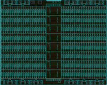
Cerebras Wafer-Scale Engine
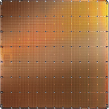
The Cerebras Wafer-Scale Engine (WSE) is undoubtedly the most bold and innovative design to appear recently. Wafer-scale integration is not a new idea, but integration issues to do with yield, power delivery and thermal expansion have made it difficult to commercialize (see the 1989Anamartic 160MBsolid state disk)). Cerebras use this approach to integrate 84 chips with high-speed interconnect, uniformly scaling the 2D-mesh based interconnect to huge proportions. This provides a machine with a large amount of memory (18GB) distributed among a large amount of compute (3.3 Peta FLOPs peak). It is unclear how this architecture scales beyond single WSEs; the current trend in neural nets is to larger networks with billions of weights, which will necessitate such scaling.
General details:
- Announced August 2019.
- 46, (mm) ************* (2) ************** (wafer-scale integrated system) (mm x) ******************************************************************************************************************************************************************* (mm) om *************** (TSMC) 16 nm.
- 1.2T transistors.
- Many individual chips: a total of 84 (12 wide by 7 tall).
- 18GBtotal ofSRAMmemory, distributed among cores.
- 426, 384 simple compute
- Silicon defects can be repaired by using redundant cores and links to bypass a faulty area. It appears that each column includes one redundant core, leaving 410, 592 functional cores.
- Speculated clock speed of ~ 1 GHz and 15 kW power consumption.
Interconnect andIO:
- Interconnections between chips, across scribe lines, with wiring added in post-processing steps after conventional wafer manufacturing.
- IOs brought out on east and west edges of wafer, which is limited by the pad density on each edge. It is unlikely there are any high-speed SerDes since these would need to be integrated in every chip, making a sizeable part of the wafer area redundant apart from chips with edges on the periphery.
- 2D mesh-based interconnect, supports single-word messages. According to their whitepaper: “The Cerebras software configures all the cores on theWSEto support the precise communication required ”indicating that the interconnect is statically configured to support a fixed communication pattern.
- Interconnect requires static configuration to support specific patterns of communication.
- Zeros not transmitted on the interconnect to optimize for sparsity.
Each core:
- ********************************** Is ~ 0.1 mm (2) of silicon.
- Has (kB) *************** (SRAM) **************** (memory.)
- Zeros not loaded from memory and zeros not multiplied.
- Assumed (FP) precision and scalar execution (can’t filter zeros from memory withSIMD).
- FMACdatapath (peak 8 operations per cycle).
- Tensor control unit to feed the (FMAC) datapath with strided accesses from memory or inbound data from links.
- Has four 8 (GB/ s bidirectional links to its neighbors.
Each die:
- Is (mm x) ********************************************************************************************************************************************************************************************************** (mm=) ************************************************************************************************************************************************* (mm) ************* (2) of silicon.
- Has 225MBSRAMmemory.
- Has 54 x 94=5, 076 cores (two cores per row / column possibly unused due to repair scheme leaving 4,
- Peak (FP) performance of 40 Tera FLOPs.
References :
- AnandTech report from (HC) , August 2019
- Cerebras white paper, August 2019 (no longer available)
- Cerebras Wafer Scale Engine: Why we need big chips for Deep Learning
Google (TPU) **************** (3)
With few details available on the specifications of theTPU3 , it is likely an incremental improvement to theTPU2: doubling the performance, addingHBM2memory to double the capacity and bandwidth.
General details:
- Announced May 2018.
- Likely to be 16 nm or 12 nm.
- (W estimated) *************** (TDP.
- 105 TFLOPs of BFloat 16, likely from doubling the MXUs to four.
- EachMXUhas dedicated access to 8 (GB) of memory.
- Integrated in four-chip modules.
IO:
- 32 (GB)HBM2integrated memory with access bandwidth of (GBps (assumed).)
- PCIe-3 x8 assumed at 8 GBps.
References :
Google (TPU) **************** (2)
TheTPU2 is designed for training and inference. It improves over theTPU1 with floating point arithmetic and enhanced memory capacity and bandwidth withHBMintegrated memory.
General details:
- Announced May 2017.
- Likely to be 20 nm.
- 200 – (W estimated) *************** (TDP) .
- 45 TFLOPs of BFloat 16.
- Two cores with scalar and matrix units .
- Also supportsFP 32.
- Integrated in four-chip modules.
Each core:
- 128 x 128 x (b systolic matrix unit)MXU) with BFloat 16 multiplication andFP 32accumulation.
- (8GB) **************** (of dedicated) *************** (HBM) with access bandwidth of (GBps.)
- Peak throughput of 22 .5 TFLOPs of BFloat 16.
IO:
- GBHBMintegrated memory at 600 GBps bandwidth (assumed).
- PCIe-3 x8 (8 GBps
References :
- NextPlatform Under The Hood Of Google’sTPU2Machine Learning Clusters, May 2017
- Tom’s Hardware: Hot Chips 2017: A Closer Look At Google’sTPUv2, September 2017
Google (TPU) **************** (1)
Google’s first generationTPUwas designed for inference only and supports only integer arithmetic. It provides acceleration to a hostCPUby being sent instructions across PCIe-3, to perform matrix multiplications and apply activation functions. This is a significant simplification which would have saved much time in design and verification.
General details:
- Announced in 2016.
- (mm) ************* (2) die on 28 nm process.
- Clocked at MHz and – WTDP.
- 28 (MB) **************** (on-chip) *************** (SRAM) memory: 24 (MB) **************** (for activations and 4) *************** (MB) for accumulators.
- Proportions of the die area: 35% memory, 24% matrix multiply unit, 41% remaining area for logic.
- (x) x8b systolic matrix multiply unit ( (K MACs / cycle).
- INT8andINT 16arithmetic (peak 92 and (TOPs / s respectively).
IO:
- ********************************** (8) *************** (GB)DDR3– 2133DRAMaccessible via two ports at 34GB/ s.
- PCIe-3 x 16 ( (GBps).
References :
- Wikipedia: Tensor Processing Unit
- (TPU) 1 paper (In-Datacenter Performance Analysis of a Tensor Processing Unit), April 2017
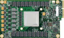
GraphcoreIPU
DISCLAIMER: I work at Graphcore, and all of the information given here is lifted directly from the linked references below.
The GraphcoreIPUarchitecture is highly parallel with a large collection of simple processors with small memories, connected by a high-bandwidth all-to-all ‘Exchange’ interconnect. The architecture operates under a bulk-synchronous parallel (BSP) model, whereby execution of a program proceeds as a sequence of compute and exchange phases. Synchronization is used to ensure all processes are ready to start exchange. TheBSPmodel is a powerful programming abstraction because it precludes concurrency hazards, andBSPexecution allows the compute and exchange phases to make full use of the chip’s power resources. Larger systems ofIPUchips can be built by connecting the (inter -) *************** (IPU) links.
General details:
- (nm, 23 .6 bn transistors, ~ 800 mm(2) ************** (die size.)
- 1216 processor tiles.
- 125 TFLOPs peakFP 16arithmetic withFP 32Accumulation.
- 300MBtotal on-chip memory, distributed among processor cores, providing an aggregate access bandwidth of
- All model state held on chip, there is no directly-attachedDRAM.
- WTDP( (W PCIe card).
IO:
- 2x PCIe-4 hostIOlinks.
- (x inter-card ‘) *************** (IPU) links’.
- Total of (GBps) *************** (IO) bandwidth.
Each core:
- Mixed-precision floating-point stochastic arithmetic.
- Runs up to six program threads.
References :
- RAAISpresentation, July 2017
- NIPSpresentation, November 2017
- ScaledML presentation, March 2018
- EETimes: GraphcoreCEOTouts’ Most Complex Processor ‘Ever, April 2019
- Serve the Home overview of the C2 card, June 2019
- WikiChip: Colossus microarchitecture
Habana Labs Gaudi
Habana’s GaudiAItraining processor shares similarities with contemporary GPUs, particularly wideSIMDparallelism andHBM2memory. The chip integrates ten (G Ethernet links which support remote direct memory access)RDMA). ThisIOcapability allows large systems to be built with commodity networking equipment, compared with Nvidia’s NVLink or OpenCAPI.
General details:
- Announced June 2019.
- TSMC16 nm with Co WoS, assumed die size ~ (m) ************* (2) .
- Heterogeneous architecture with:
- aGEMMoperations engine;
- 8 Tensor Processing Cores (TPCs)
- a sharedSRAMmemory (software managed and accessible viaRDMA).
- 200 WTDPfor PCIe card and 300 WTDPfor the mezzanine card.
- Unknown total on-chip memory.
- Explicit memory management between chips (no
TPCcore:
- VLIWSIMD (parallelism and a local) *************** (SRAM) **************** (memory.)
- Mixed precision: (FP) , (BF) , plus integer formats ( (INT) , (INT) ,INT8,UINT 32,UINT8).
- Random number generation.
- Transcendental functions: Sigmoid, Tanh, Gaussian error linear unit (GeLU).
- Tensor addressing and strided access.
- Unknown local memory perTPC.
IO:
- ********************************** (4x) HBM2- 2000DRAMstacks providing 32 (GB) at 1 TBps.
- 10 x 100 GbE interfaces are integrated on-chip , supportingRDMAover Converged Ethernet (RoCE v2).
- IOs are implemented with 20 x (Gbps) *************** (PAM4) **************** (Tx / Rx SerDes and can also be configured as) x 50 GbE. This allows up to 64 chips to be connected with non-blocking throughput.
- PCIe-4 x 16 host interface.
References :
- The Next Platform:AIChip Startup Releases Training Accelerator to Challenge GPUs , June 2019
- AnandTech report fromHC 31, August 2019
- Habana Labs Gaudi whitepaper, August 2019
Huawei Ascend 910
Huawei’s Ascend also bears similarities to the latest GPUs with wideSIMDarithmetic and a 3D matrix unit, comparable to Nvidia’s Tensor Cores, a (assumed) coherent 32MBshared L2 on-chip cache. The chip includes additional logic for 128 channel video decoding engines for H. 264 / 265. In their Hot Chips presentation, Huawei described overlapping the cube and vector operations to obtain high efficiency and the challenge of the memory hierarchy with ratio of bandwidth to throughput dropping by 10 x for L1 cache (in the core), 100 x for L2 cache (shared between cores), and (x for external) *************** (DRAM) .
General details:
- Announced August 2019.
- (mm) 2logic die on a 7 nmEUVprocess.
- Copackaged with four (mm) ************* (2)HBM2stacks and ‘Nimbus’ (IO) processor chip.
- (DaVinci cores.)
- Peak (TFLOPs) (x) ************************************************************************************************************** (x 2)FP 16performance, double that forINT8.
- 32MBshared on-chip (SRAM) **************** (L2 cache).
- (W) *************** (TDP) ****************.
Interconnect andIO:
- Cores interconnected in a 6 x 4 2D mesh packet-switched network, providing 128 GBps bidirectional bandwidth per core.
- 4 TBps access to L2 cache.
- 1.2 TBpsHBM2access bandwidth.
- 3x 30 GBps inter -chip IOs.
- 2x 25 GBps RoCE networking interfaces.
Each DaVinci core:
- ********************************** (3D) ********************************************************************************************************************************************************************************************************************** (x) ********************************************************************************************************************************************************************************************************************** (x) matrix multiply unit providing 4.0 96FP 16MACs and 8, 192INT8MACs.
- 2, (bit) *************** (SIMD) **************** (vector operations for) *************** (FP) (x 64),FP 16(x 128) andINT8(x 256).
- Support for scalar operations.
References :
IntelNNP– T
This chip is Intel’s second attempt at an accelerator for machine learning, following the Xeon Phi. Like theHabana Gaudi chip, it integrates a small number of wide vector cores, withHBM2integrated memory and similar (Gbit) *************** (IO) links.
General details:
- 27 BN transistors.
- 688 mm2die onTSMC16 FFTSMCwith CoWoS.
- 32 (GB) (HBM2) – 2400 in four 8GBstacks integrated on a (mm) ************* (2) ************** (passive silicon interposer.)
- 60MBon-chipSRAMmemory distributed among cores andECCprotected.
- Up to 1.1 GHz core clock.
- 150 – (W) *************** (TDP) .
- (Tensor Processing Cluster)TCP(cores.)
- TPCs connected in a 2D mesh network topology.
- Separate networks for different types of data: control, memory and inter -chip communication.
- Support for multicast.
IO:
- ********************************** 1. (TBps) *************** (HBM2) bandwidth.
TPCcore:
- ********************************** (2x) x BFloat multiplier arrays supportingFMAC (operation with) *************** (FP)accumulation.
- Vector (FP) and BFloat 16 operations.
- Support for transcendental functions, random number generation, reductions and accumulations.
- Programmable (FP) lookup tables.
Scaling :
- Up to 1024 chips with direct interconnections, providing the same distributed-memory programming model (explicit memory management,
- Scaling demonstrated up to 32 chips connected in a ring topology.
References:
- WikiChip: Intel’s Spring CrestNNP-L Initial Details, April 2019
- Tom’s Hardware, August 2019
- (Intel’s) *************** (HC) presentation (PDF), August 2019
- AnandTech report fromHC 31, August 2019
Nvidia Volta
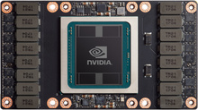
Volta introduces Tensor Cores,HBM2and NVLink 2.0, from ThePascal architecture.
General details:
- Announced May 2017.
- (mm) ************* (2) onTSMC(nm) FFN, 21. 1 BN transistors.
- 300 WTDP(SXM2form factor).
- 6 (MB) L2 cache.
- 84 SMs, each containing: 64FP 32CUDAcores, 32 (FP)CUDAcores and 8 Tensor Cores (5376FP 32cores , 2688FP 64cores, (TCs).
- Tensor Cores perform 4×4FMA, achieving 64FMA ops / cycle, and 128 FLOPs.
- 128KB (L1 data cache / shared memory and four) ********************************************************************************************************************************************************************************************************************** (K) – bit registers perSM.
IO:
- 32 (GB)HBM2DRAM, at 900 GBps bandwidth.
- NVLink 2.0 at 300 GBps.
References :
- Wikipedia: Volta (microarchitecture)
- Volta architecture whitepaper
- (Nvidia Tesla V) datasheet
- AnandTech –NVIDIAVolta Unveiled:GV 100(GPU) and Tesla V 100 Accelerator Announced , May 2017
Nvidia Turing
Turing is an architectural revision of Volta, manufactured on the same 16 nm process, but with fewerCUDAand Tensor cores. It consequently has a smaller die size and lower power envelope. Apart fromMLtasks, it is designed to perform real-time ray tracing, for which it also used the Tensor Cores.
General details:
- Announced September 2018.
- TSMC(nm) FFN, (mm) ************* (2) die, 18 .6 BN transistors.
- (W) TDP.
- 72 SMs, each containing: 64FP 32cores, and 64INT 32cores, 8 Tensor cores (4608FP 32cores, 4608INT 32 (cores and 576 TCs .
- Peak performance with boost clock: 16 3 TFLOPsFP 32, 5 TFLOPs *************** (FP) , 261 TFLOPsINT8, (TFLOPs) *************** (INT4) .
- 24 .5MBon-chip memory between 6 (MB) L2 cache and 256KBSMregister files.
- (MHz base clock.)
IO:
- (x) – bitGDDR6memory providing 672 GBps aggregate bandwidth.
- 2x NVLink x8 links, each providing up to 26 GBps bidirectional.
References :
- Wikipedia: Turing (mircoarchitecture)
- (AnandTech:) *************** (NVIDIA) **************** (Reveals Next-Gen Turing) *************** (GPU) Architecture, August 2018
- Nvidia TuringGPUarchitecture whitepaper (PDF)
Further reading
- AIChip – A list of ICs and IPs for (AI) , Machine Learning and Deep Learning (GitHub)
- (MLPerf Training v0.6 results)TPU3and Volta only)
Please get in touch (mail @ this domain) with any comments, corrections or suggestions.

(Read More)
GIPHY App Key not set. Please check settings